I – Sensor part of an instrumental chain
1 – R&D electric field sensor
CNES funding was obtained for this R&D action which is part of the preparation of tomorrow’s scientific instruments for electric field measurement (upstream technological research, mastery of micro-technologies). The objective was to propose a microsystem solution for the measurement of electric field in the frequency range from DC to 1 kHz. The MEMS solution allowed a direct measurement of the electric field and a very small footprint.
The LPC2E has been developing for several years short electrical antennas for the measurement of alternating fields from a few kHz to several tens of MHz. The last realization of the LPC2E was embarked in 2004 on the cometary probe ROSETTA.
Several R&D actions have been carried out in recent years to improve the performance of electric antennas, such as the ASIC solution of the high input impedance preamplifier (see R&D electric antenna preamplifier). No major improvement seems possible without a strong technical breakthrough. With this R&T, we have studied the possibility to make a direct measurement of the field, while current sensors (antenna) deduce the field from a potential difference between two monopoles.
Preliminary studies were carried out at the LPC2E in the framework of master 2 internships, on the one hand, to validate the theoretical aspect of the sensor and, on the other hand, to imagine and simulate an architectural concept allowing to answer our specifications. The results obtained have encouraged us to continue in this direction. The research continued through a CNES R&T funding and a thesis grant in cotutelle with IRIS industrie. The thesis allowed to establish international collaborations with the University of Louvain la Neuve in Belgium and national collaborations with the IEMN laboratory in Lille and the CMP in Grenoble. The funding of the scholarship was provided by the Loiret General Council CG 45. The thesis of Mr Boujhrarhe was defended in 2013. This work has led to the filing of a patent and publications.
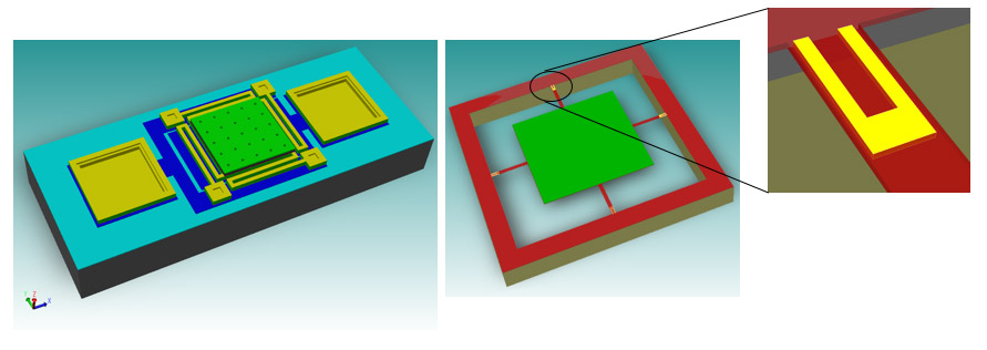
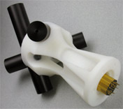
MEMS architecture of the electric field sensor (G) capacitive architecture, (D) piezoresistor-based architecture
A prototype of the sensor was manufactured at the IEMN. This foundry allowed to validate the theoretical operation of the sensor as shown in the figures below.
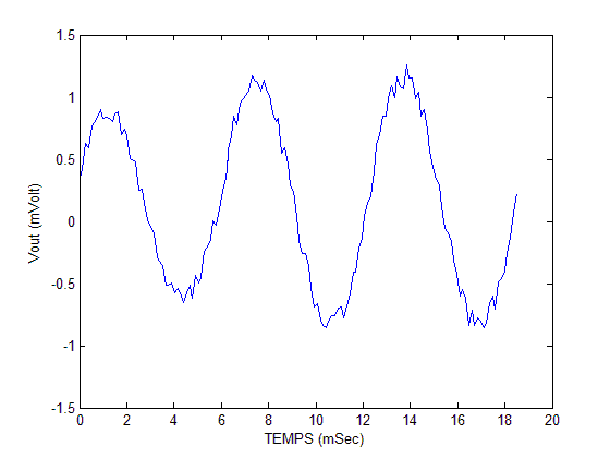
(a) Transient response of the sensor for an excitation of 1 mV/m at a frequency of 170 Hz
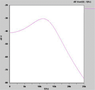
(b) Response of the sensor to a variation in the frequency of the excitation signal fixed at 1 mV/m.
In AC, the sensor “follows” the evolution of the excitation signal but with a phase shift (sensor response time), figure (a). The prototype allows to measure a weak field up to 2.8×10⁻⁵ V/m. The response of the sensor “remains” flat from DC to the first pole around 11 kHz, figure (b).
2 – R&D magnetic field sensor
This action has been funded by CNES and is part of the preparation of future scientific instruments for the measurement of broadband magnetic field. The objective is to propose a microsystem solution for the measurement of the magnetic field from a few Hz to 50 kHz. The microsystem solution will eventually replace search coil type sensors (400 g, 20 cm in diameter), a great miniaturization and a very small footprint.
Within the framework of its research on the ionized environments of the planets of the solar system, the LPC2E has been developing for a certain number of years electrical and magnetic sensors intended to be embarked on satellites or interplanetary probes. Although performing (sensitivity of a few fT/Hz1/2 in VLF-MF) and answering perfectly to the request concerning the reliability, they remain relatively heavy and cumbersome, which implies relatively heavy and often complex deployment systems. Examples include the integration of a triaxial search coil sensor on the DEMETER satellite in 2004 and on the future TARANIS mission planned for 2018. Several R&T actions have been carried out in recent years to reduce the size and improve the performance of search coil sensors, such as reducing the size of the magnetic bars and miniaturizing the receiving electronics. However, no major improvement now seems to be possible without a strong technical breakthrough. Indeed, the operating principle of this sensor is based on induction and we are reaching the limits (in terms of sensitivity) of what this technique can allow. The emergence of new MEMS technologies as well as techniques based on thin films and especially “spintronics”, allow us to envisage in the near future much lighter and less bulky sensors. Within the framework of an R&T for which we obtained a CNES funding, we have conducted for a few years an in-depth study on giant magnetoresistors (GMR), with the aim of developing a sensor of a few cm³ and weighing a few grams, while having performances close to those developed so far. Although the results obtained are encouraging (size, weight and bulk) we have not managed to achieve performances (sensitivity, noise) similar to those of the search-coil.
This work is currently under the responsibility of a CNRS engineer from LPC2E who continued the developments using this time a SDT (Spin Dependent Tunneling) sensor. These new developments have led to the MAROT project.
3 – R&D Improvement of the response of a ceramic piezoelectric sensor
This action took place upstream of the R&D electric field sensor. Indeed, during the exploration of new technologies and sensors that could allow us to develop a miniaturized electric field sensor, we were interested in piezoelectric sensors. Although the piezoelectric solution was not chosen for the development of our sensor, we have nevertheless developed a polarization method that improves the electrical response of piezoelectric sensors when they are subjected to mechanical excitation.
Indeed, the recovery of mechanical vibration energy from the environment to convert it into electrical energy is the key to develop autonomous sensor systems. To do this study, we have created a parametric FEM model of piezoelectric sensor. This model, developed under Comsol environment, allowed to validate our polarization concept. The concept was validated experimentally on a test bench. The polarization has thus improved the response of piezoelectric sensors, in our case it was a sensor in the form of ceramic lamellae, by a factor of 18% while reducing the risk of destruction of the lamellae. This work led to two publications.
4 – R&D Cooled sensors (superconductors) for space applications
At very low temperatures, the electrical and magnetic properties of certain materials such as lead, mercury or certain oxides change radically. These materials become superconductors: they no longer offer any resistance to the passage of electric current and expel magnetic fields.
Superconductors are already used in many fields: electricity, medicine and even in space. They are also at the heart of laboratories, in particle accelerators, in the field of astrophysics with bolometers, in ultra-sensitive magnetic sensors such as SQUIDs, or to produce very intense magnetic fields. However, they need to be cooled to very low temperatures.
In this study, we have discussed the relevance of using cooled sensors in the space domain. We have given a snapshot of recent developments in superconducting materials, cooled sensors for space, technologies for cold generation/production, and we have listed all the space missions that could carry them.
This R&D has led to a publication and a contract with ALCATEL Space for which we have provided a prospecting report on this technology for future space missions.
II – Amplifier part of an instrumental chain
1 -R&D Low temperature ASIC preamplifier for search-coil sensor
The objective of this R&D is to develop a preamplifier in ASIC technology allowing the operation of the LF 10Hz-20KHz search-coil instrument in a wide temperature range.
The LPC2E conducts research activities on the ionized environment of the Earth, planets and the Sun-Earth relationship. The ESPACE team is engaged in the realization of instruments in various international projects: Solar Orbiter and Parker Solar Probe dedicated to the study of the Sun.
Solar Orbiter (SO) and Parker Solar Probe (PSP) are respectively missions of ESA and NASA. Among the scientific objectives of these missions are the study of the acceleration of the solar wind, the heating of the solar corona and the acceleration of cosmic rays of solar origin. The participation of the LPC2E to these missions is done through the instruments RPW-SCM for SO and SCM for PSP. They are both tri-axial magnetometers of the search-coil type.
The development of search-coil magnetometers is an essential activity of the ESPACE team at LPC2E. However, each mission has different constraints and specifications regarding radiation resistance, power consumption and temperature. For the SO and PSP missions, the scientific instrumentation is placed behind a heat shield to protect the scientific payload from very high temperatures. Nevertheless, the instruments are still subjected to a temperature gradient varying between -150° C and 100° C.
Search-coil with preamp integrated in the foot
The electronics of the search coil magnetometer currently provided by the LPC2E operates in a temperature range between -50°C and 80°C. In practice, this limitation forces the search coils onboard for these missions to have a heating line in order to be able to operate at low temperatures. This heating line alone consumes 2W while the instrument consumes 270 mW for a ±12V supply!!!
To address this problem, a low-temperature preamplifier R&D started in September 2018 (for more details see the research outlook section).
2 – R&D preamplifier for electrical antennas
The aim was to develop a very high input impedance, low noise preamplifier in ASIC technology. The objective was to improve the measurement of the electric field by using electric antennas as sensors. This R&D study financed by the CNES allowed to design a BiCMOS ASIC circuit in AMS 0.8 µm technology. The foundry was carried out via the CMP Grenoble. The circuit thus obtained was successfully tested, partly under tip at the radio astronomy station of Nançay. This work has been published.
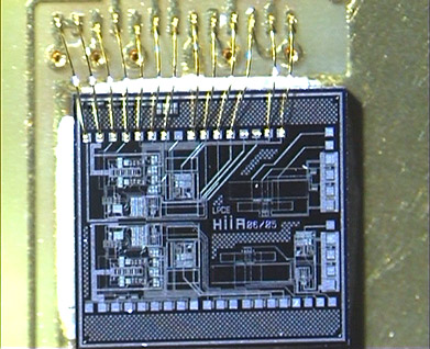
High input impedance ASIC preamplifier for the TARANIS mission. Y. Kebbati (LPC2E, 2005)
III – Analog to digital converter part of the instrumental chain
1 – R&D Improved resolution of analog/digital converters
As part of a feasibility study, we have developed a new technique to improve the resolution of analog-to-digital converters. This technique is based on the statistical principle “bootstrap”. The algorithm has been validated in Matlab and the hardware architecture described in VHDL. An FPGA synthesis under MaxplusII environment has been done in order to evaluate the hardware performances of our algorithm. This study led to two publications.
2- R&D Improved resolution of analog/digital converters
In this work, we have developed a method allowing the use of a low resolution analog to digital converter in a high resolution instrumental chain. Indeed, the use of a high resolution ADC increases the cost of the instrumental chain and limits the bandwidth of the signals that can be processed. Based on this observation, we have developed a method based on the interpolation of the signal from the converter. This study allowed us to improve the resolution of a 12-bit ADC by making it work like a 16-bit ADC. The interpolation algorithm has been implemented on Altera’s FPGA Cyclone V target. This work led to the supervision of two master internships and two publications.
IV – Digital processing part, by ASIC/FPGA integration, of the instrumental chain
1 – Development of a hardware design methodology based on generic VHDL/VHDL-AMS modules for the integration of electrical control systems
In spite of their flexibility and economic interest, digital solutions of software type implementation are no longer the only choice for electrical system control design. Indeed, more specific hardware solutions (FPGA, ASIC) seem to better meet the current or future technological constraints. However, despite the advent of tools and powerful CAD languages, these solutions are still too expensive and complex to implement. The objective of the work carried out is to offer to the designers of electrical systems an approach of architectural description adapted to the constraints of implementation on a target material. Thus, a method based on the principles of the modular design of Algorithm Architecture Adequacy and on the elaboration of a library of specific modules could be developed for various cases of control. Thus, the architecture of the direct torque control of an asynchronous motor could be established following this method and its efficiency could be validated by comparing its implementation performances to those of more classical design approaches. Subsequently, the case of a “sensorless” speed control of a variable reluctance motor and that of a power electronics device were also able to show the effectiveness of the proposed method. From this last design case, a global methodology of the modular design mode could finally be elaborated by developing a library of behavioral models of the control and the associated electrical system. These models have been described in VHDL and VHDL-AMS languages in order to respect the mix (digital and analog) of the elements that compose the electrical system. This approach also allows to foresee the case of a mixed integration of the system, opening by the same way wide perspectives of design in this application domain. This work has been the subject of several publications and communications.
2- R&D RSFQ logic (superconductors) for space applications
Since the discovery of superconductivity and the Josephson junction (JJ) in the 1960s, a new area of microelectronics has emerged. Indeed, the current superconducting integrated circuits use the inherent characteristics of the JJ to achieve performances (data processing speed at high frequency, low power dissipation…) previously unmatched by CMOS circuits. These characteristics can be summarized:
– Availability of microstrip superconducting transmission lines capable of transferring picosecond waves with a speed approaching that of light.
– JJs can be used as ultrafast (picosecond) switch/memory.
– JJs can be easily impedance matched with microstrip lines which allows ballistic transfer of the generated waves. Thus, JJs have a very low power dissipation due to the low voltages used.
The RSFQ elementary element consists of an interferometer composed of a Josephson diode coupled with a superconducting inductive element and Josephson diode-based transmission lines. This architecture allows the transfer or storage of a logic pulse (magnetic flux quanta) without attenuation or distortion at frequencies of several hundred gigahertz (750 GHz) and with an extremely low power consumption (< 100 nW/gate). In addition, unlike JJ, RSFQ circuits require only a DC power supply. Furthermore, compared to current CMOS technology, they use a relatively simple fabrication technology that does not require deep submicron design.
The state of the art of RSFQ logic shows that this technology is viable for different application domains. Indeed, we are witnessing in recent years, a significant increase in the number of circuits developed and performance achieved (speed, power consumption, integration density) and the emergence of new technologies: new JJ, submicron technology … In the space domain, the generation of cold remains a problematic lock and this technology has not yet found its place despite the growing needs in computing power. This R&D has led to a contract with ALCATEL Space for which we have provided a report on the use of RSFQ logic for future space missions. This work led to a publication.
Research prospects
I – Medium-term perspective (≤ 5 years)
Development of an LF search-coil instrument with digital output that can operate in a temperature range of -150° C to 100° C.
The objective of the study is to develop a 10 Hz – 20 kHz LF search-coil magnetometer instrument with digital output of the plug&play type and able to operate in a wide temperature range between -150° C and 100° C. For this purpose, a development of an adapted electronics will be necessary. To achieve our goal, we will use microelectronic technology to integrate the electronic instrumental chain of the search-coil: preamplifier, filter and analog-to-digital converter. The developments will be done in three main steps:
– ASIC integration of the search-coil preamplifier for operation between -150°C and 100°C (see: R&D low temperature preamplifier for search-coil)
– Development of a 16bits ASIC CAN and filter
– Integration of the whole electronic chain.
Collaborations
This study will be done through the supervision of a thesis in collaboration with the IRFU laboratory of CEA Saclay which already has experience in low temperature ASIC developments. The ASIC circuit foundries will be done through the CMP or Europractice networks in order to reduce development costs by taking advantage of prices dedicated to universities and research.
Technological locks
The choice of technology and encapsulation are the main obstacles in this R&D.
The technology will have a direct impact on the performance of the circuits and will make it possible to reach our objective of operating at low temperatures (150°C). Indeed, current technologies are designed for operation between -50°C and 80°C. Thus, an in-depth technological study phase will be necessary. This study will take the form of a first foundry dedicated to basic circuits. The goal is that after the tests of return of foundry, a finer modeling of the operation of transistors in low temperature will be then possible. This will allow to complete the models provided by the foundry. We expect that the developments will probably be done in AMS 0.35 µm technology because this technology is now both widespread, robust (available for several years) and low cost. However, we will remain attentive to the latest advances in microelectronics before choosing the appropriate technology to achieve our goal.
Encapsulation is a recurring problem in space and the low temperatures we want to reach only increase the constraints. It will therefore be necessary to take this problem into account from the beginning of the design of the circuits in order not to alter the performance after the foundry and, on the other hand, for the transfer of the chip to the PCB. Indeed, in the case of the LPC2E search-coil magnetometer instrument, the pre-amplification electronics are generally located in the foot of the search-coil sensor.
Contact LPC2E : Youssef.Kebbati@cnrs-orleans.fr